- 您现在的位置:买卖IC网 > Sheet目录3854 > PIC18F86J15-I/PT (Microchip Technology)IC PIC MCU FLASH 48KX16 80TQFP
PIC18F87J10 FAMILY
DS39663F-page 28
2009 Microchip Technology Inc.
2.2
Power Supply Pins
2.2.1
DECOUPLING CAPACITORS
The use of decoupling capacitors on every pair of
power supply pins, such as VDD, VSS, AVDD and
AVSS, is required.
Consider the following criteria when using decoupling
capacitors:
Value and type of capacitor: A 0.1
μF (100 nF),
10-20V capacitor is recommended. The capacitor
should be a low-ESR device with a resonance
frequency in the range of 200 MHz and higher.
Ceramic capacitors are recommended.
Placement on the printed circuit board: The
decoupling capacitors should be placed as close
to the pins as possible. It is recommended to
place the capacitors on the same side of the
board as the device. If space is constricted, the
capacitor can be placed on another layer on the
PCB using a via; however, ensure that the trace
length from the pin to the capacitor is no greater
than 0.25 inch (6 mm).
Handling high-frequency noise: If the board is
experiencing high-frequency noise (upward of
tens of MHz), add a second ceramic type capaci-
tor in parallel to the above described decoupling
capacitor. The value of the second capacitor can
be in the range of 0.01
μF to 0.001 μF. Place this
second capacitor next to each primary decoupling
capacitor. In high-speed circuit designs, consider
implementing a decade pair of capacitances as
close to the power and ground pins as possible
(e.g., 0.1
μF in parallel with 0.001 μF).
Maximizing performance: On the board layout
from the power supply circuit, run the power and
return traces to the decoupling capacitors first,
and then to the device pins. This ensures that the
decoupling capacitors are first in the power chain.
Equally important is to keep the trace length
between the capacitor and the power pins to
a minimum, thereby reducing PCB trace
inductance.
2.2.2
TANK CAPACITORS
On boards with power traces running longer than six
inches in length, it is suggested to use a tank capacitor
for integrated circuits including microcontrollers to
supply a local power source. The value of the tank
capacitor should be determined based on the trace
resistance that connects the power supply source to
the device and the maximum current drawn by the
device in the application. In other words, select the tank
capacitor so that it meets the acceptable voltage sag at
the device. Typical values range from 4.7
μF to 47 μF.
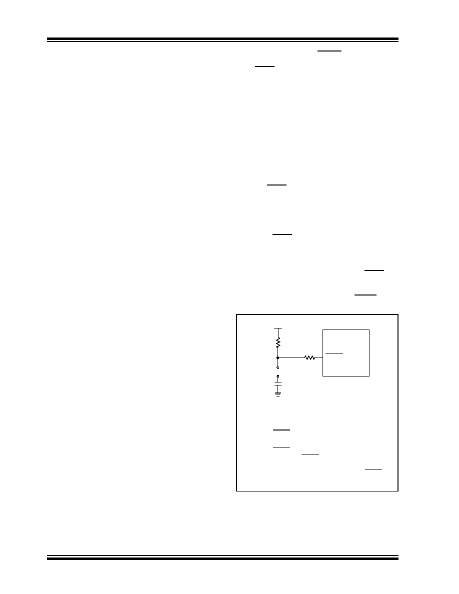
2.3
Master Clear (MCLR) Pin
The MCLR pin provides two specific device
functions: device Reset, and device programming
and debugging. If programming and debugging are
not required in the end application, a direct
connection to VDD may be all that is required. The
addition of other components, to help increase the
application’s resistance to spurious Resets from
voltage
sags,
may
be
beneficial.
A
typical
configuration is shown in Figure 2-1. Other circuit
designs may be implemented depending on the
application’s requirements.
During programming and debugging, the resistance
and capacitance that can be added to the pin must
be considered. Device programmers and debuggers
drive the MCLR pin. Consequently, specific voltage
levels (VIH and VIL) and fast signal transitions must
not be adversely affected. Therefore, specific values
of R1 and C1 will need to be adjusted based on the
application and PCB requirements. For example, it is
recommended that the capacitor, C1, be isolated
from the MCLR pin during programming and
debugging operations by using a jumper (Figure 2-2).
The
jumper
is
replaced
for
normal
run-time
operations.
Any components associated with the MCLR pin
should be placed within 0.25 inch (6 mm) of the pin.
FIGURE 2-2:
EXAMPLE OF MCLR PIN
CONNECTIONS
Note 1: R1
≤ 10 kΩ is recommended. A suggested
starting value is 10 k
Ω. Ensure that the
MCLR pin VIH and VIL specifications are met.
2: R2
≤ 470Ω will limit any current flowing into
MCLR from the external capacitor, C, in the
event of MCLR pin breakdown, due to
Electrostatic Discharge (ESD) or Electrical
Overstress (EOS). Ensure that the MCLR pin
VIH and VIL specifications are met.
C1
R2
R1
VDD
MCLR
PIC18FXXJXX
JP
发布紧急采购,3分钟左右您将得到回复。
相关PDF资料
ATMEGA16-16AC
IC AVR MCU 16K 16MHZ COM 44-TQFP
ATMEGA16-16MC
IC AVR MCU 16K 16MHZ COM 44-QFN
ATMEGA16-16PC
IC AVR MCU 16K 16MHZ COM 40-DIP
ATMEGA128L-8MI
IC AVR MCU 128K LV 8MHZ IND64QFN
ATMEGA128L-8MC
IC AVR MCU 128K LV 8MHZ COM64QFN
25FMN-BMTTN-A-TF
CONN FMN HSNG 25POS STAG NOR SMD
23FMN-BMTTN-A-TF
CONN FMN HSNG 23POS STAG NOR SMD
22FMN-BMTTN-A-TF
CONN FMN HSNG 22POS STAG NOR SMD
相关代理商/技术参数
PIC18F86J15T-I/PT
功能描述:8位微控制器 -MCU 96 KB FL 4 KB RAM RoHS:否 制造商:Silicon Labs 核心:8051 处理器系列:C8051F39x 数据总线宽度:8 bit 最大时钟频率:50 MHz 程序存储器大小:16 KB 数据 RAM 大小:1 KB 片上 ADC:Yes 工作电源电压:1.8 V to 3.6 V 工作温度范围:- 40 C to + 105 C 封装 / 箱体:QFN-20 安装风格:SMD/SMT
PIC18F86J16-I/PT
功能描述:8位微控制器 -MCU 96KB FL 3936b RAM 10 MIPS 67 I/O RoHS:否 制造商:Silicon Labs 核心:8051 处理器系列:C8051F39x 数据总线宽度:8 bit 最大时钟频率:50 MHz 程序存储器大小:16 KB 数据 RAM 大小:1 KB 片上 ADC:Yes 工作电源电压:1.8 V to 3.6 V 工作温度范围:- 40 C to + 105 C 封装 / 箱体:QFN-20 安装风格:SMD/SMT
PIC18F86J16T-I/PT
功能描述:8位微控制器 -MCU 96KB Flash 3936bytes RAM 67 I/O RoHS:否 制造商:Silicon Labs 核心:8051 处理器系列:C8051F39x 数据总线宽度:8 bit 最大时钟频率:50 MHz 程序存储器大小:16 KB 数据 RAM 大小:1 KB 片上 ADC:Yes 工作电源电压:1.8 V to 3.6 V 工作温度范围:- 40 C to + 105 C 封装 / 箱体:QFN-20 安装风格:SMD/SMT
PIC18F86J50-I/PT
功能描述:8位微控制器 -MCU 64KB Flash 3936byte RAM RoHS:否 制造商:Silicon Labs 核心:8051 处理器系列:C8051F39x 数据总线宽度:8 bit 最大时钟频率:50 MHz 程序存储器大小:16 KB 数据 RAM 大小:1 KB 片上 ADC:Yes 工作电源电压:1.8 V to 3.6 V 工作温度范围:- 40 C to + 105 C 封装 / 箱体:QFN-20 安装风格:SMD/SMT
PIC18F86J50T-I/PT
功能描述:8位微控制器 -MCU 64KB FLSH 3936Bs RAM USB 2.0 nanoWatt RoHS:否 制造商:Silicon Labs 核心:8051 处理器系列:C8051F39x 数据总线宽度:8 bit 最大时钟频率:50 MHz 程序存储器大小:16 KB 数据 RAM 大小:1 KB 片上 ADC:Yes 工作电源电压:1.8 V to 3.6 V 工作温度范围:- 40 C to + 105 C 封装 / 箱体:QFN-20 安装风格:SMD/SMT
PIC18F86J55-I/PT
功能描述:8位微控制器 -MCU 96KB FLSH 3936Bs RAM USB 2.0 nanoWatt RoHS:否 制造商:Silicon Labs 核心:8051 处理器系列:C8051F39x 数据总线宽度:8 bit 最大时钟频率:50 MHz 程序存储器大小:16 KB 数据 RAM 大小:1 KB 片上 ADC:Yes 工作电源电压:1.8 V to 3.6 V 工作温度范围:- 40 C to + 105 C 封装 / 箱体:QFN-20 安装风格:SMD/SMT
PIC18F86J55T-I/PT
功能描述:8位微控制器 -MCU 96KB FLSH 3936Bs RAM USB 2.0 nanoWatt RoHS:否 制造商:Silicon Labs 核心:8051 处理器系列:C8051F39x 数据总线宽度:8 bit 最大时钟频率:50 MHz 程序存储器大小:16 KB 数据 RAM 大小:1 KB 片上 ADC:Yes 工作电源电压:1.8 V to 3.6 V 工作温度范围:- 40 C to + 105 C 封装 / 箱体:QFN-20 安装风格:SMD/SMT
PIC18F86J60-I/PT
功能描述:8位微控制器 -MCU 64KB FL 12KB RAM 10BASE-T RoHS:否 制造商:Silicon Labs 核心:8051 处理器系列:C8051F39x 数据总线宽度:8 bit 最大时钟频率:50 MHz 程序存储器大小:16 KB 数据 RAM 大小:1 KB 片上 ADC:Yes 工作电源电压:1.8 V to 3.6 V 工作温度范围:- 40 C to + 105 C 封装 / 箱体:QFN-20 安装风格:SMD/SMT